
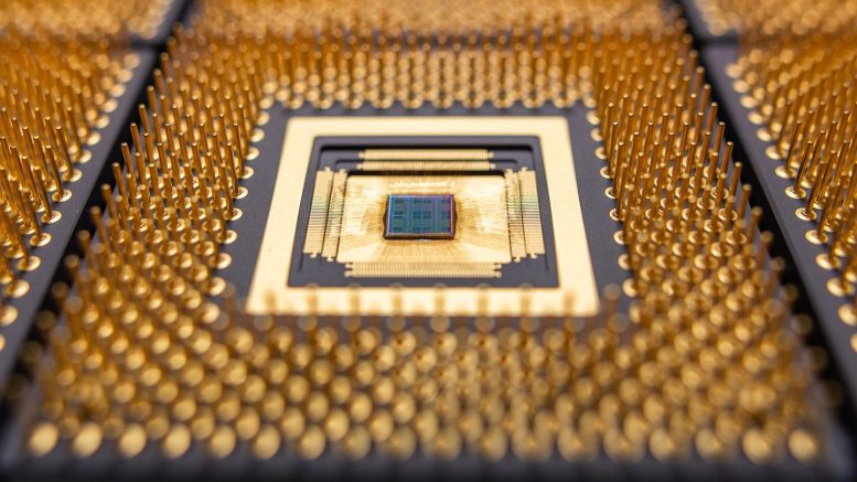
Princeton University researchers have reimagined the entire physics of computing to build a chip for modern AI workloads, and with new support from the U.S. government, they'll see how fast, small and power-efficient this chip can be. An early prototype is pictured above. Credit: Hongyang Jia/Princeton University
The Advanced Artificial Intelligence Chip Project at Princeton, powered by… DARPA and EnCharge AI, promise significant improvements in energy efficiency and computing power, aiming to revolutionize the accessibility and application of AI.
The Department of Defense's largest research organization has partnered with a Princeton-led effort to develop advanced microchips for artificial intelligence.
New devices reimagine AI chips for modern workloads and can run powerful AI systems using significantly less power than today's most advanced systems. SemiconductorsAccording to Naveen Verma, professor of electrical and computer engineering. Verma, who will lead the project, said the developments break through key barriers that have held back AI chips, including size, efficiency and scalability.
Revolutionizing the deployment of artificial intelligence
Chips that require less power to power AI can be deployed in more dynamic environments, from laptops and phones to hospitals and highways to low Earth orbit and beyond. The types of chips that power today's most advanced models are too bulky and inefficient to run on small machines, and are primarily limited to server racks and large data centers.
Now, the Defense Advanced Research Projects Agency, or DARPA, has announced that it will support Verma's work, based on a set of key inventions from his lab, with an $18.6 million grant. DARPA's funding will lead to exploration of how fast, small and energy efficient the new chip can get.
“There is a very important limitation that the best AI available is only in the data center,” Verma said. “You unleash that, and I think the ways in which we can get value from AI will explode.”
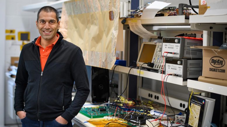
Professor Naveen Verma will lead a US-backed project to enhance artificial intelligence devices based on a set of key inventions from his laboratory at Princeton. Credit: Samir A. khan/photobody
The announcement came as part of a broader effort by DARPA to fund “revolutionary advances in science, devices and systems” for the next generation of artificial intelligence computing. The program, called OPTIMA, includes projects across multiple universities and companies. The program's call for proposals estimated total funding at $78 million, though DARPA has not disclosed the full list of institutions or the total amount of funding the program has awarded yet.
The advent of EnCharge AI
In the Princeton-led project, researchers will collaborate with Verma's startup EnCharge AI. EnCharge AI is based in Santa Clara, California, and commercializes technologies based on discoveries from Fermat's lab, including several key research papers he has co-written with electrical engineering graduate students since 2016.
Encharge AI “brings leadership in the development and implementation of robust and scalable mixed-signal computing architectures,” according to the project proposal. Verma co-founded the company in 2022 with Kailash Gopalakrishnan, a former IBM colleague, and Ishiri Iruaga, a leading semiconductor systems designer.
Innovation in existing computing architectures, as well as improvements in silicon technology, is beginning to slow as artificial intelligence begins to create massive new demands on computational power and efficiency, Gopalakrishnan said. Not even the best graphics processing unit (GPU), used to power current AI systems, can alleviate the bottlenecks in memory and computing power facing the industry.
“Although GPUs are the best tool available today, we concluded that a new type of chip would be needed to unleash the potential of AI,” he said.
Transforming the AI computing landscape
Between 2012 and 2022, the amount of computing power required by AI models has increased by about 1 million percent, according to Verma, who is also director of the Keller Center for Innovation in Engineering Education at UCLA. Princeton University. To meet demand, the latest chips are assembled into tens of billions of transistors, each separated by a small width. virus. However, chips are still not dense enough in their computing power to meet modern needs.
Today's leading models, which combine large language models with computer vision and other methods Machine learning, developed using over a trillion variables each. Nvidia-designed graphics processing units that fueled the AI boom have become so valuable that major companies are said to be transporting them in armored cars. The backlog to buy or lease these chips is stretching to the vanishing point.
When Nvidia became only the third company ever to reach $2 trillion, the Wall Street Journal reported that a rapidly growing share of the company's growing revenues came not through developing models, called training, but in chips that enable artificial intelligence systems to be used. Once she is already trained. Technologists refer to this deployment phase as heuristics. Heuristics is where Verma says his research will have the greatest impact in the near to medium term.
“It's all about decentralizing AI and unleashing it from the data center,” he said. “We have to move out of the data center and into places where we and the processes that matter most have access to computing, which are phones and laptops and factories and things like that.”
Innovating artificial intelligence chip technology
To create chips that can handle modern AI workloads in embedded or power-constrained environments, researchers had to completely reimagine the physics of computing while designing and packaging devices that can be made using current manufacturing techniques and that can work well with existing computing technologies. Like the CPU.
“AI models have evolved tremendously, and that means two things,” Verma said. AI chips must become more efficient at performing calculations and more efficient at managing and transmitting data.
Their approach consists of three main parts.
The basic architecture of almost every digital computer has followed a deceptively simple pattern first developed in the 1940s: store data in one place, perform calculations in another. This means transferring information between memory cells and the processor. Over the past decade, Verma has pioneered research into an updated approach where calculations are done directly in memory cells, called in-memory computing. This is the first part. The promise is that in-memory computing will reduce the time and energy it takes to transfer and process large amounts of data.
But until now, digital approaches to in-memory computing have been very limited. Verma and his team turned to an alternative approach: analog computation. This is the second part.
“With in-memory computing, not only do you need to do the computing efficiently, you also need to do it at a very high density because they now need to fit into these very small memory cells,” Verma said. Instead of encoding information in a series of 0s and 1s, and processing that information using traditional logic circuits, analog computers take advantage of the richer physics of the devices. Gear curvature. The ability of a wire to retain an electrical charge.
Digital signals began to replace analog signals in the 1940s, primarily because binary code evolved better with the explosive growth of computing. But digital signals don't delve into the physics of the devices and, as a result, can require more data storage and management. They are less efficient this way. Analog gets its efficiency from precise signal processing using the intrinsic physics of the devices. But this can come with a trade-off in accuracy.
“The key is to find the right physics for the task in a device that can be very well controlled and manufactured at scale,” Verma said.
His team has found a way to perform extremely precise calculations using the analog signal generated by capacitors specially designed to turn on and off with extreme precision. This is the third part. Unlike semiconductor devices such as transistors, the electrical energy moving through capacitors does not depend on variable conditions such as temperature and electron movement in the material.
“They just rely on engineering,” Verma said. “It depends on the distance between one metal wire and the other metal wire.” Engineering is one of the things that today's most advanced semiconductor manufacturing technologies can control very well.